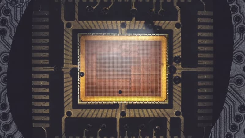
A hobbyist called Breaking Taps has fabricated a custom microprocessor using wafer.space, a commercial IC fabrication service, and documented the entire process on video. The chip is a transport-triggered architecture design with two buses, built-in memory, and peripherals, making it closer to a system-on-chip than a bare processor. He used Spade, an HDL, to design it, and the finished die is visible under clear epoxy in a chip carrier package, mounted on a PCB and running real programs.
The chip uses older fabrication technology, which is why the die is physically large compared to modern standards. Unlike Tiny Tapeout, which tiles multiple designs on a shared cell-based wafer, this is a single-circuit chip occupying the full space. The gap between passing DRC on a PCB and getting silicon back from a fab is vast, and the video covers that gap in detail: this is where the article earns its read.
wafer.space is not cheap, and this remains a tool for well-funded individuals or small teams, not casual tinkerers. But the trajectory matters. Tiny Tapeout, wafer.space, and similar services have compressed what once required a corporate budget into something a determined engineer can attempt. The floor is still dropping.
[READ ORIGINAL →]