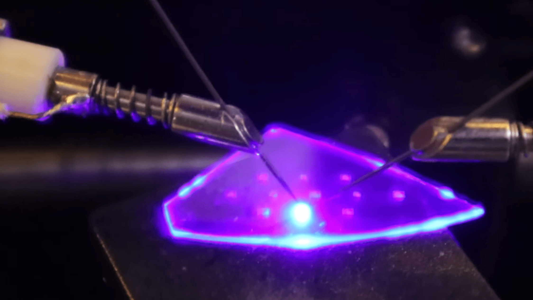
A hobbyist known as Dr. Semiconductor has fabricated functional GaN LEDs from scratch and flip-chip bonded them to a PCB using electroplated indium bumps, rosin flux, and reflow soldering. The starting material is a commercial GaN epiwafer: n-doped GaN, an indium gallium nitride quantum well layer, and p-doped GaN on a sapphire substrate. Applying current produces bright blue light. This is not a demonstration. It is a repeatable home fab process with a working assembly at the end.
The process details are where this piece earns a full read. Exposing the n-type contact layer normally requires reactive ion etching in chlorine, industrial equipment most hobbyists cannot access. Dr. Semiconductor replaced that step with a 355-nm UV laser to decompose GaN into gallium and nitrogen, followed by a potassium hydroxide cleanup etch. Metal contacts of nickel, silver, and titanium were then deposited via sputtering through a photoresist lift-off mask. To convert the blue output to white, he applied cerium-doped yttrium aluminium garnet phosphor powder suspended in clear silicone directly over the bonded chip.
The broader goal is flip-chip bonding of opaque silicon devices to PCBs, a significant alignment challenge. The transparent GaN LED served as the alignment trial run, and it worked. Dr. Semiconductor is actively developing the next stage of that process. The original guide at semiconductor.diy walks through every step, and the embedded video shows the chip lighting up on the board.
[READ ORIGINAL →]